
This is the third part of a four-part post detailing the design, manufacture, and programming of a reflow oven based on the Panasonic NT-GT1, 9-liter, 1200W toaster oven:
- 1 (Oven hardware)
- 2 (Controller hardware)
- 3 (Manufacturing)
- 4 (Controller software)
So far we’ve looked at the hardware design, but aside from modifying the oven in part 1, nothing has been built yet.
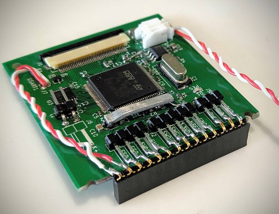
PCB
You’ll find JLC PCB reviews and links all over the Internet thanks to them providing discounts to anyone willing to write a testimonial. I’ve used them in the past and never had any serious issues, although my designs are generally not pushing any boundaries.
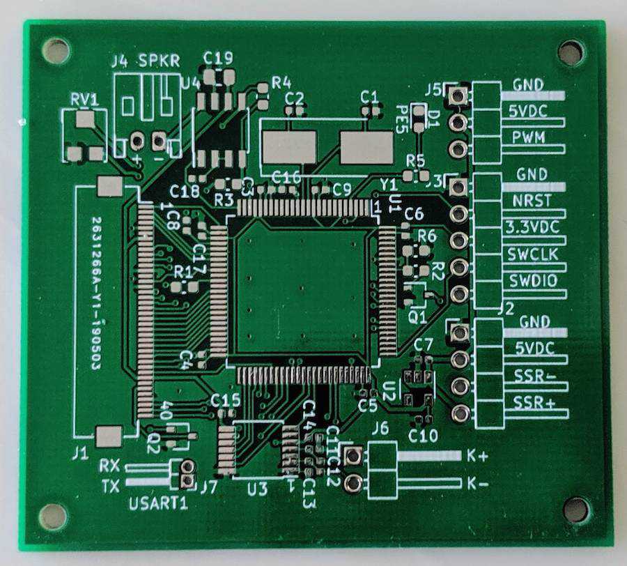
I plotted out the gerbers, sent them off, and after a few days, the boards arrived looking very much like the KiCad 3D renders
Despite having only one board to build, I ordered a stencil. I didn’t much fancy applying paste by hand for the 100-pin MCU package or the 40-pin TFT connector (both 0.5 mm pitch).
I don’t really like steel stencils. I often find them to be too thick for <=0.5 mm pitch parts, resulting in too much paste on the pads and resulting bridges. Perhaps I’ve just been unlucky with suppliers, but I’ve never had these problems with plastics. Unfortunately JLC only have steel on offer and only in a single thickness.
Assembly
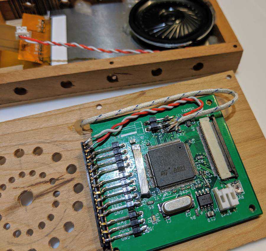
How do you reflow the board for a controller in a reflow oven? You use the same oven with a human controller of course. After applying paste and placing the components, I hooked the thermocouple up to a multimeter to monitor the temperature and manually cycled the oven power via the SSR in an attempt to follow the profile as closely as possible.
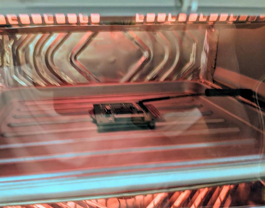
Reflowing the controller board in the oven
As predicted, the stencil was a bit thick for 0.5mm pitch components, and several bridges needed to be manually fixed. Once the SMD side was done, the through hole components were soldered into position.
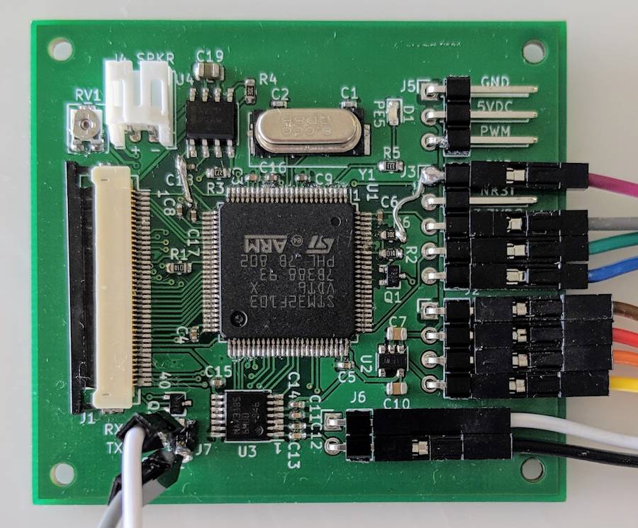
Soldered controller board showing manual fixes for two board errors described below
PCB errors and things I would have done differently
Straight up PCB errors
- RX/TX silkscreen reversed
- Missing ground connection in 2 places
Placement of the thermocouple IC and connection was less than ideal
Thermocouples work by producing a voltage that is proportional (but not linearly so) to the temperature difference along it’s length. Thus in order to know the absolute temperature at the business end, it’s necessary to know the absolute temperature at the cold end - the “reference” junction.
This reference junction is the point at which the special metals of the thermocouple terminate.
Thermocouple ICs like the MAX31856 have internal temperature sensors for this purpose. For accurate readings, there must be no unknown or varying thermal gradient (i.e. temperature difference) between the IC and the reference junction. A fixed difference can be accounted for.
Without much consideration for how much heat the 3.3V regulator would be producing (quite a lot it turns out given that it’s powering the TFT LCD backlight), I had placed the MAX31856 nearby and the thermocouple connector between them.
Although we’re not measuring the CMB temperature, errors of more than a couple of degrees still have the potential to cause problems.
To mitigate the issue, I made two modifications:
- Rotated the thermocouple connector 180° so that it lies directly above the MAX31856.
- Installed a heatsink on the regulator and oriented it away from the thermocouple area.
The heatsink is a short piece of aluminum that I cut off a fan grill and glued to the top of the regulator using JB Weld, which I’m led to believe from random forum posts is a not too terrible conductor of heat.
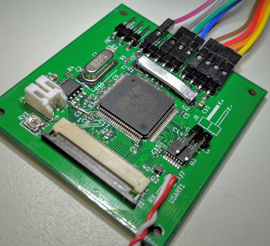
Controller board with thermocouple fixes (heatsink and flipped connector)
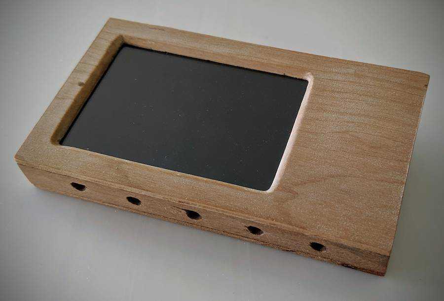
Enclosure
Enclosures for one-off projects are a pain. Absent a CNC machine, high-end 3D printer (+ lots of sanding, painting etc.), making an enclosure that doesn’t look like a high school science fair project is difficult. For this project, I’ve gone with wood.
I don’t own any power tools suitable for use at this scale, but thin, softish wood (cherry in this case) can be easily worked with a knife and file.
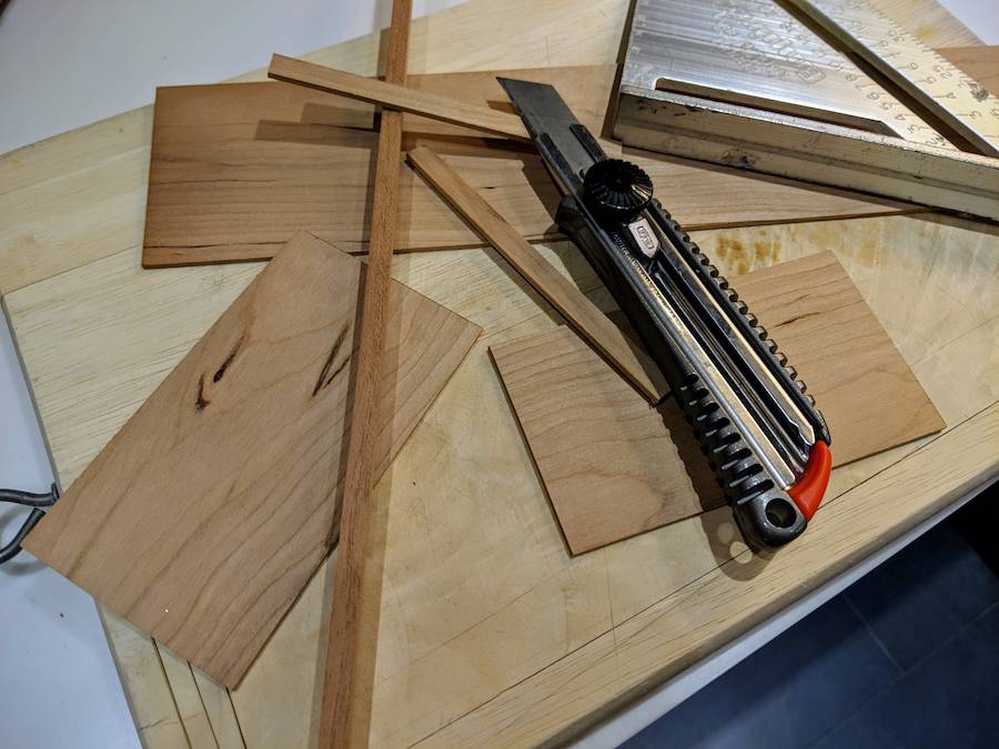
Wood for the enclosure
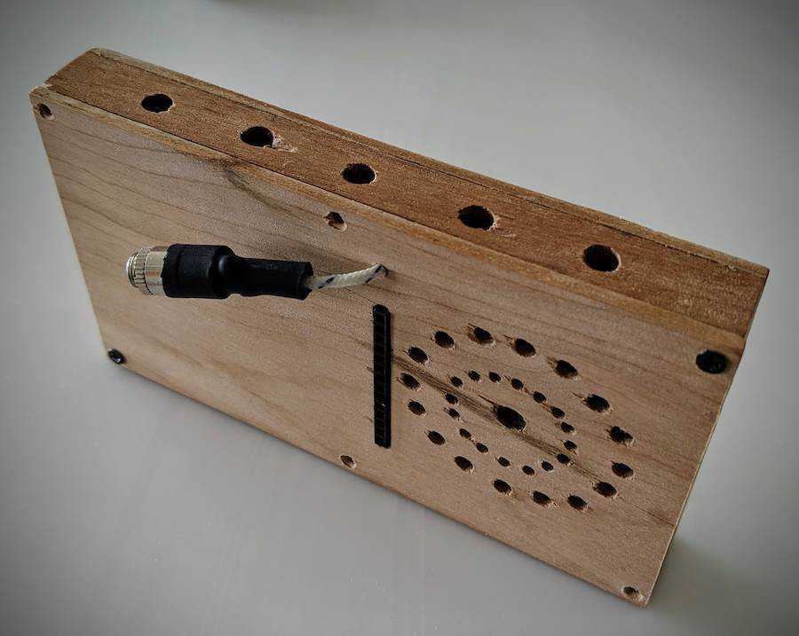
Enclosure I/O
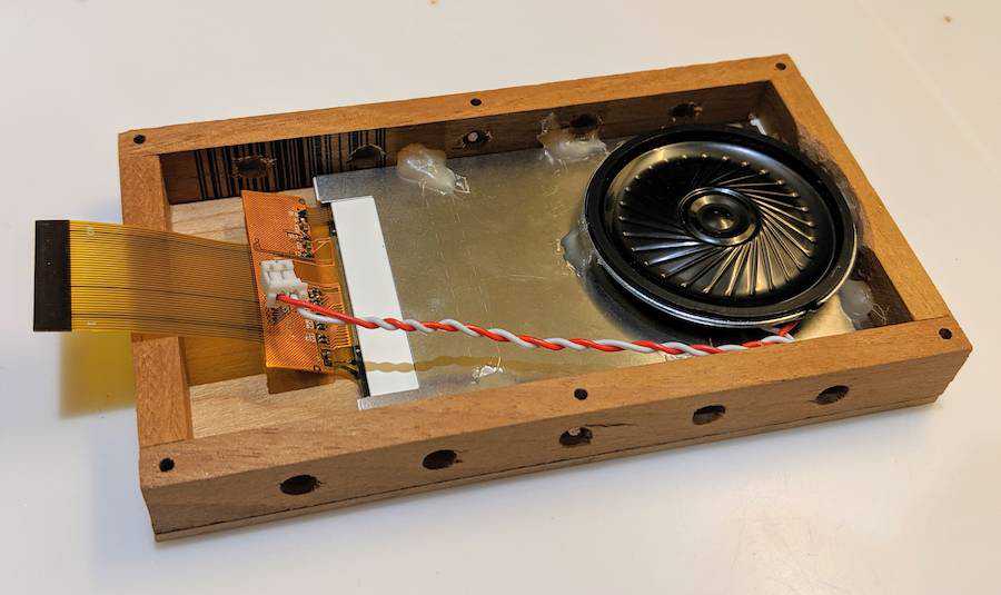
I hadn’t really thought out the enclosure situation when I designed the board. I placed pin headers on the board edge and assumed I’d run a single fat cable through a cable gland, plus the thermocouple. After designing and mostly building the enclosure, that didn’t seem like such a great option; in particular since so many of the connections would be used rarely if at all (SWD, USART etc.).
If I’d worked all this out up front, I would have put a socket on the board that protrudes through the enclosure.
Using what I had on hand, I soldered a single row, female pin-header onto (and at right-angle to) the existing pin header.
Modified I/O connector to protrude through the enclosure
This then fits into a thin slit cut in the back of the enclosure and sits flush with the outer surface. I printed out a label and glued it down next to the header for easy reference.
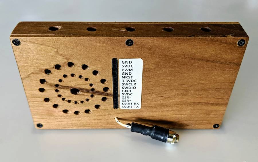
Labeled I/O connector on rear of enclosure
That’s the hardware side done. Next up, the software.