This is the second part of a six-part post:
Circuit design and prototyping
The prior post already detailed the key electronic components choices. Putting all of these together:
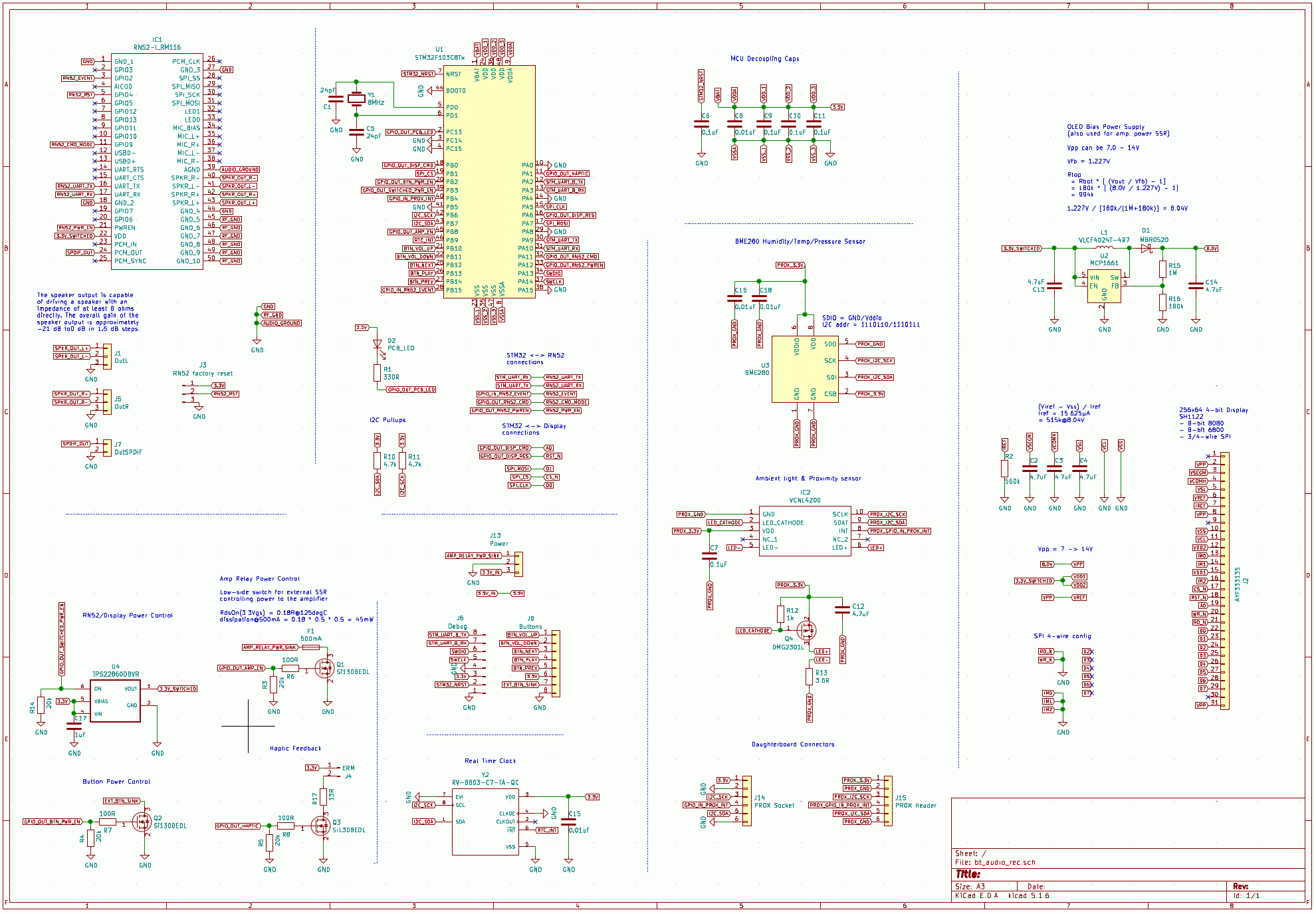
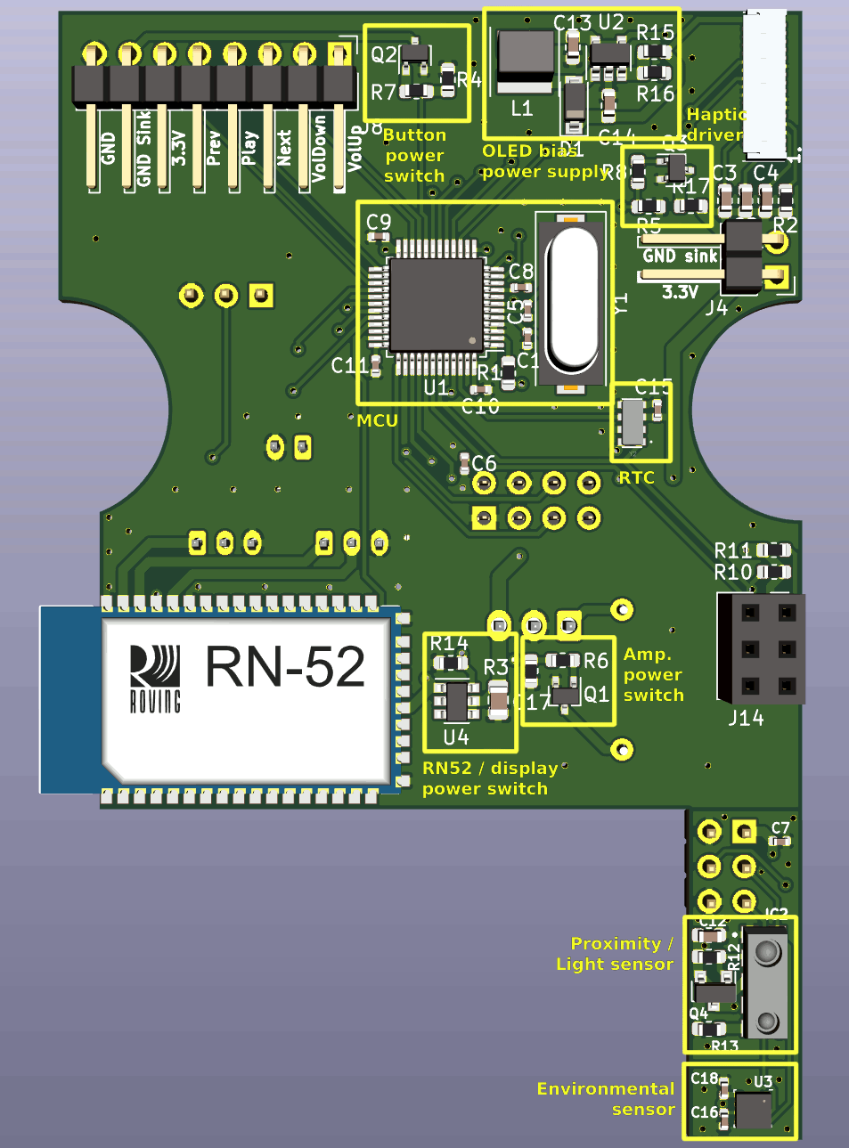
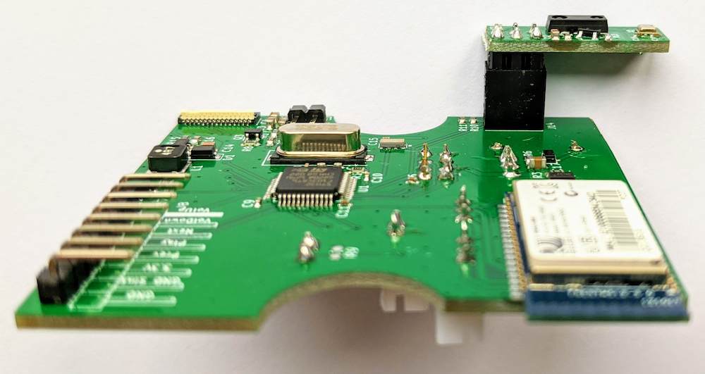
The circuit design is not complicated. The main sections are:
- MCU with 8MHz crystal and supporting caps.
- The RN52 with serial connection to the MCU
- The OLED display connected to the MCU over SPI.
- OLED 8V boost power supply.
- Environmental, ambient light, proximity sensors and RTC connected to the MCU over I2C.
- Several logic-controled “switches” to isolate power to specific devices. Primarily MOSTFETs, but one high-side switching IC.
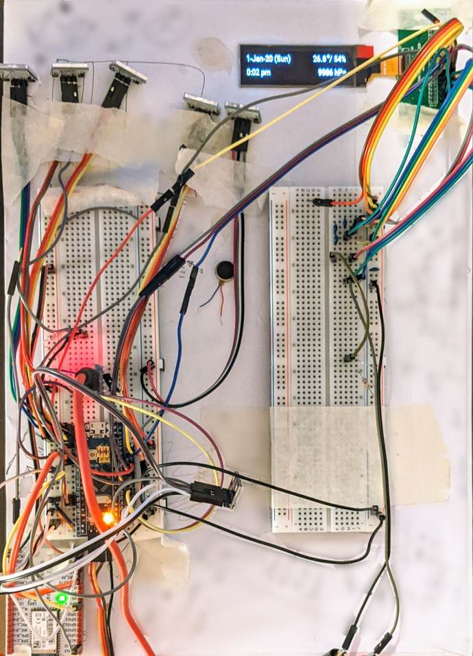
Firmware development was primarily done on a prototype design
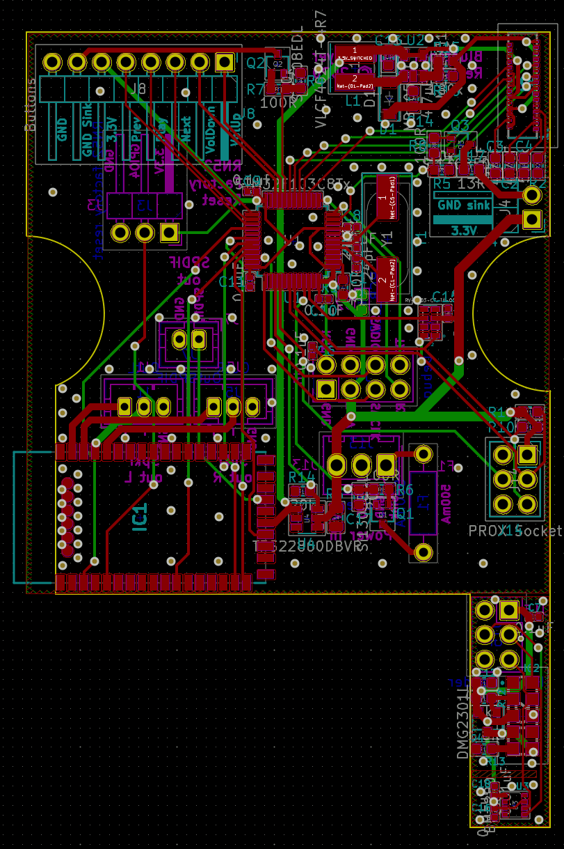
PCB design
The PCB was one of the more mechanically constrained designs I have done (see next post). The most pressing constraints were:
- Alignment requirements between the screen’s FPC connection and the proximity/light sensor daughterboard
- Bluetooth antenna location
- Analog audio routing, and
- Capacitive button connections
There is plenty of real estate on the board, but the functional layout was challenging.
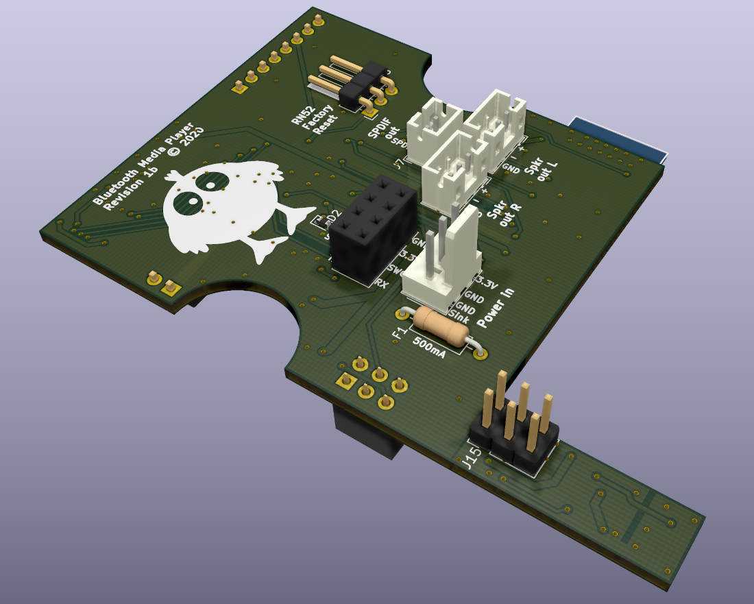
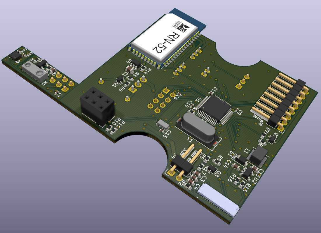
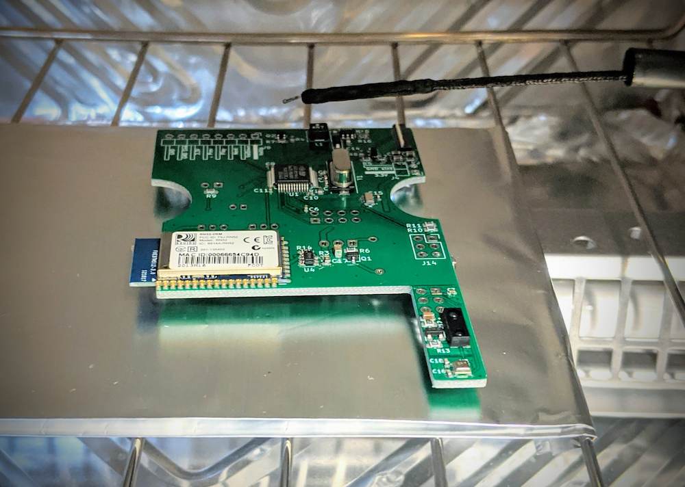
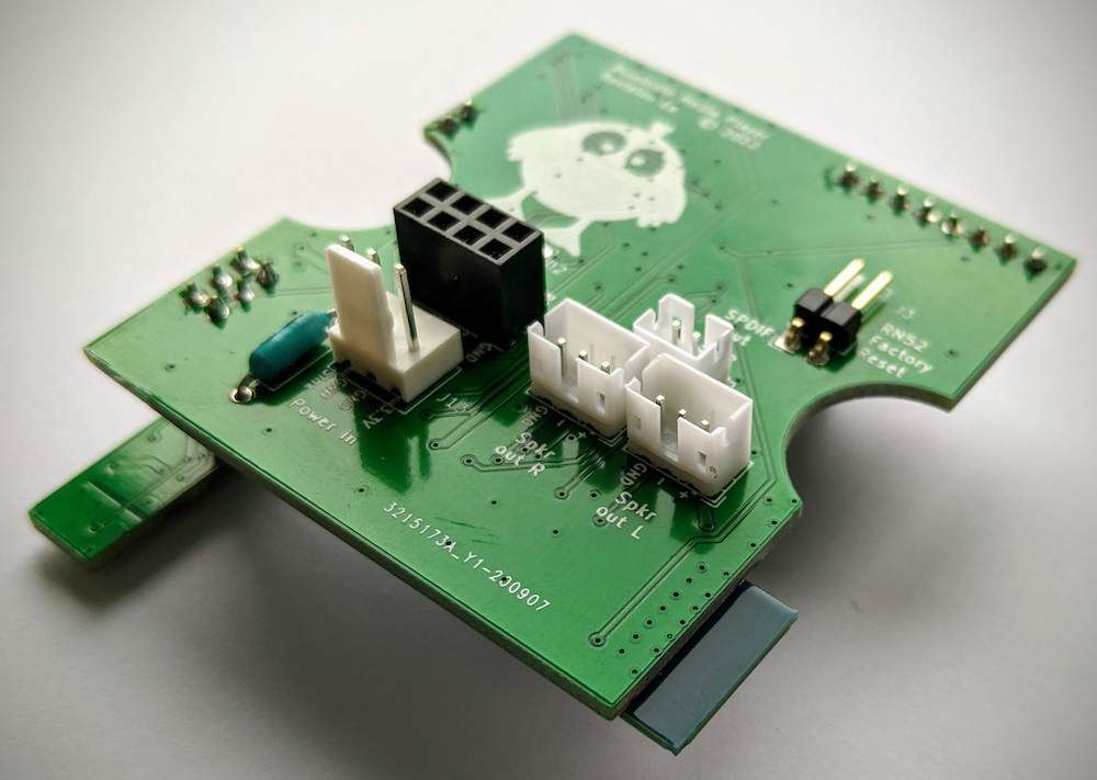
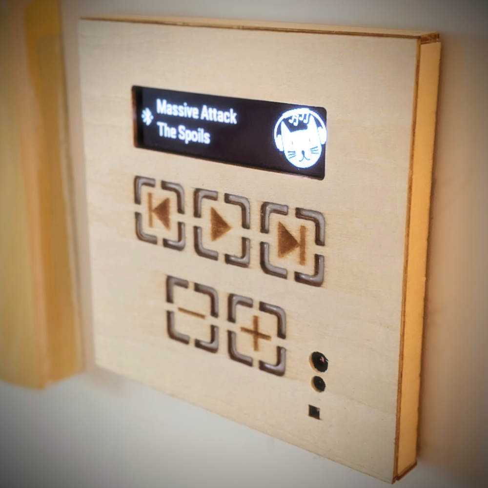
Below are the design images and the actual assembled board, which was reflowed in my toaster reflow oven.
The finger-like piece extending out the side of the PCB is the daughterboard, which is separated after fabrication and mounted via a connector, as seen the final images below. The next post describes the mechanical design behind this.