This is the second part of a four-part post detailing the design, manufacture, and programming of a reflow oven based on the Panasonic NT-GT1, 9-liter, 1200W toaster oven:
- 1 (Oven hardware)
- 2 (Controller hardware)
- 3 (Manufacturing)
- 4 (Controller software)
In part 1 we discussed the selection and modification of the oven itself. It’s now time to work on the external controller.
The primary controller hardware components are:
- LCD touch screen for input and output.
- Power supply.
- Audio amplifier and speaker for audio feedback.
- Thermocouple amplifier/encoder.
- LCD backlight brightness driver.
- SSR driver.
- A microcontroller to manage everything.
- Enclosure to house all of the above.
- A servo to open/close the oven door.
The design looks something like this:
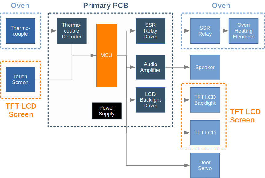
Complete system design
Core electronic blocks
Thermocouple encoder
The K-type thermocouple we’re using produces a small voltage dependent on the temperature. This voltage represents the different in temperature between the measuring end of the thermocouple and the opposite end (AKA the cold junction) and doesn’t vary linearly with temperature. Some processing is thus required to linearize the signal as well as adjust for the temperature of the cold junction.
This could theoretically be done by the MCU using one of its ADCs, a temperature sensor, and some basic code, but it’s vastly simpler and likely a lot more accurate to use a dedicated thermocouple-to-digital signal converter.
We’re using the MAX31856, which will perform digitization, linearization and cold-junction compensation, and send the data as degrees Celcius to the MCU via SPI.
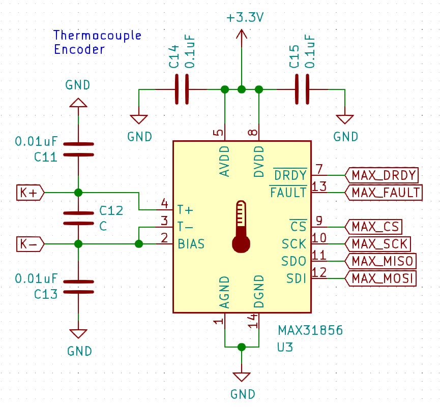
Thermocouple encoder circuit schematic
Audio amplifier
A speaker will be included for feedback when pressing the touchscreen and to signal bake/reflow completion or error conditions. It’s typical to use a piezo based device to produce short beeps and buzzes, but since they’re boring, we’ll be using a proper speaker in combination with the MCU’s DAC to replicate classic arcade game sounds.
The MCU’s DAC is unable to drive a speaker directly - an amplifier or buffer is required. A discrete circuit would work, but doesn’t make much sense when a dedicated 1W class A/B IC is only US$0.50. We’re using the ON Semiconductor NCS2211.
Calculating the correct gain
The speaker being used is 32Ω and is rated at 0.25W (presumably RMS). We can therefore drive it at a maximum of 2.8VRMS
Vrms = √(power * resistance)
     = √(0.25 * 32)
     = 2.83V
Vref for the DAC is set to 3.3V. The maximum amplitude of the DAC audio output is thus:
Vpeak = 3.3V / 2
      = 1.65V

Vrms = 1.65V / √2
     = 1.17V
And so the maximum gain (AVD) we can safely use is:
= output amplitude / input amplitude
= 2.83 / 1.17
= 2.42
The actual gain in the circuit is limited to about 1.5 by the fact that we only have a 5V supply (= 5.0 / 3.3). The gain is set by R3 and R4:
Avd = 2 * R4 / R3
Avd = 2 * 20 / 27
Avd = 1.48
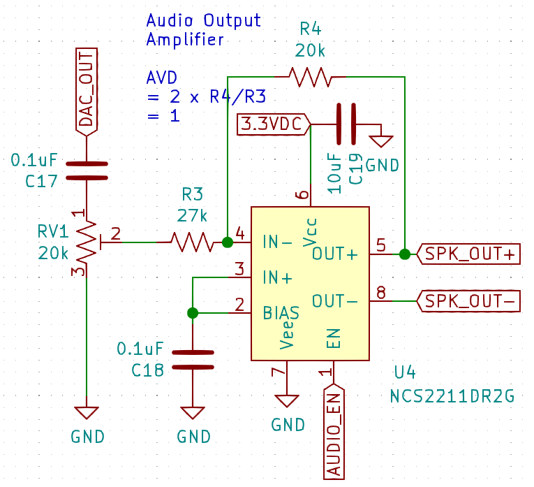
Audio amplifier circuit schematic
SSR driver
The SSR has a minimum drive voltage of 4VDC and a maximum drive current of 20 mA. The MCU will be operating at 3.3V, and so even before considering the maximum GPIO output current, its clear that an output buffer/switch is needed. A simple MOSFET switch using the Vishay Si1308EDL N-channel MOSFET will suffice. This MOSFET has an Rds(on) of 0.185Ω at a Vgs of 2.5V and drain current of 1.3A, so it will be dissipating a few milliwatts at most.
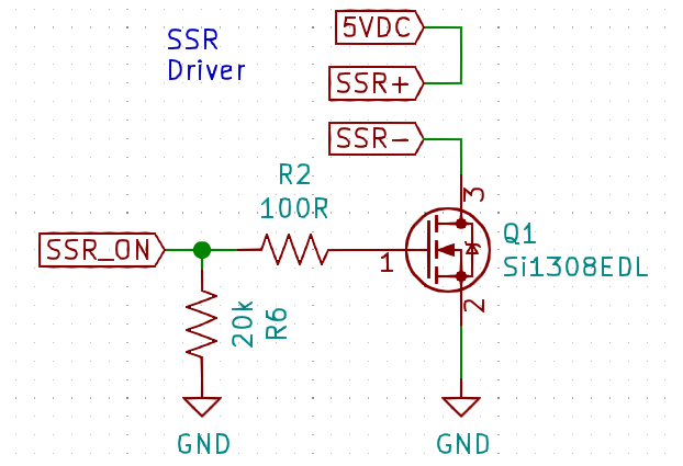
SSR driver circuit schematic
R2 isn’t really required given the slow switching frequency and low gate capacitance of the MOSFET, but it wont hurt.
R6 is important as it prevents the SSR (and thus the heating elements) from turning on when the MCU output is floating (during power up/reset or malfunction).
LCD backlight driver
The TFT LCD module is a 3.5" 320x480 device with integrated controller (ILI9481), touchscreen and backlight obtained from a no-name seller on Aliexpress.
As will all things Aliexpress, documentation is less than stellar, consisting of a single page with the FPC pinout and a schematic showing six LEDs connected to a common anode and six cathodes. That’s all well and good, but with only three cathodes on the FPC cable, it’s a little hard to trust.
Testing shows the three cathodes connected together and infinite resistance between the cathode and anode in either direction, which shouldn’t be the case if the LEDs are wired as shown. Since the FPC pinout indicates that the anode should be driven 3.0 - 3.4V, it seems likely that the device already has some sort of driver for the LEDs. Driving it at 3.3V consumes about 60mA, which seems reasonable.
To control the brightness, we’ll use a PWM signal from the MCU to switch the LEDs on/off via a MOSFET. The circuit is largely the same as the SSR driver above. excluding the safety pull-down.
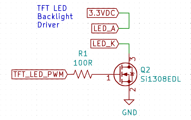
LED backlight driver circuit schematic
Power supply
The power requirements are modest:
3.3VDC@100mAfor the MCU+PCB LED5Vfor the door opening servo- >
4VDC@20mAfor the SSR 3.3VDC@100mAfor the TFT LED backlight
With a regulated 5VDC 600mA supply from the oven, we can setup a 3.3V regulator for the MCU and backlight and use the 5VDC for everything else.
The 3.3V regulator is the Texas Instruments TLV755P. It’s a pretty typical 500mA LDO (thermal shutdown, current limit, UVLO etc.), is available in a variety of fixed output voltages, and will operate with a 1uF output cap. It costs ~$0.20 at quantity.
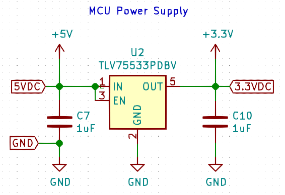
Power supply circuit schematic
Input / Output
TFT LCD display module
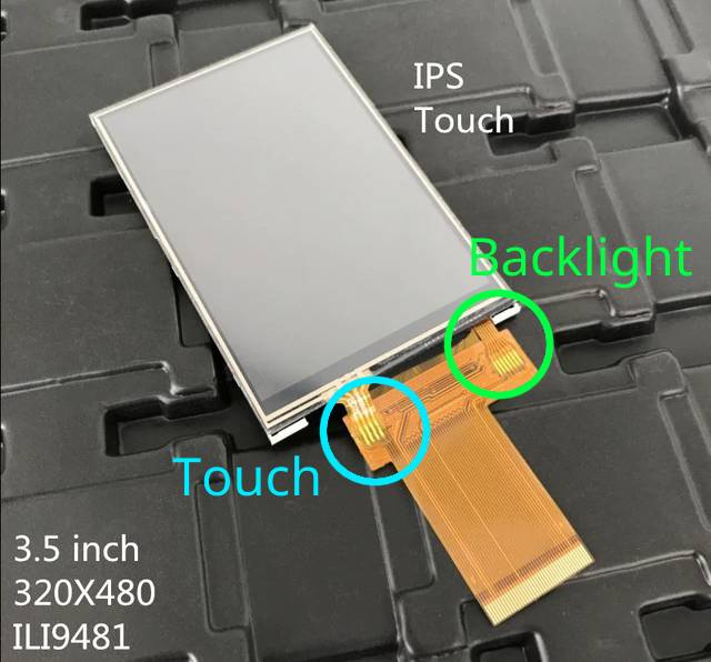
3.5’ 480x320 TFT display used in the project
As mentioned above, the display is a 3.5" 480x320x16-bit TFT LCD with an ILI9481 controller, integrated resistive touch screen, backlight, and uses a 40-pin FPC connector. The ILI9481 supports a few different interfaces, including 18-bit parallel, but the module is only wired for a 16-bit bus, so I’ll be using 16-bit parallel DBI.
Touch screens simplify the input hardware and software
Managing input via dedicated buttons is mechanically challenging and generally more expensive than touch screen input. I prefer buttons in many situations, but for this application, a touch screen offers a better UI.
Touch screens come in capacitive or resistive varieties. Resistive touch screens are very simple devices. They are basically just two big, transparent, square resistors sitting on top of each other.
By connecting one edge of one sheet to ground and the opposite edge of the same sheet to a set potential (e.g. Vcc)*, a linear voltage gradient is setup across it. If the other sheet is left unconnected, then when it is pressed, it becomes electrically connected to powered sheet at the point of touch and so it’s voltage will be equal to that of the powered sheet at that point. Measuring this voltage via an ADC tells us the relative distance from the grounded and powered edges.
This gives us the position in one dimension. Switching the sheets and repeating the process using the other edges gives us the other dimension.
To facilitate this measurement, a typical panel provides electrical connections for the left and right edges of one sheet and the top and bottom edges of the other. They are usually labeled X negative, X positive, Y negative, Y positive, although left/right/top/bottom/up/down or other nomenclature may be used.
* We don’t need to use ground or Vcc, the only thing that matters is that we have a potential difference across the sheet and known potentials at either edge.
From a practical perspective with an MCU, the process to determine touch screen position goes something like this:
-
Connect one of the sheets to ground (either edge), connect the other to an input with a pullup, wait until it is pulled low (i.e. from a touch).
-
Connect the left edge of the X sheet to ground and the right edge to Vcc, measure the voltage on one edge of sheet Y via an ADC for our X position.
-
Connect the top edge of the Y sheet to ground and the bottom edge to Vcc, measure the voltage on one edge of sheet X via an ADC for our Y position.
There are additional steps available to determine the pressure of the touch and reliable detection requires some software filtering, but this is the basic process.
Overall Control - the MCU
Selecting an appropriate microcontroller
Choosing a microcontroller for a project is always a challenging task, primarily because there are so many similar products from competing vendors (and even from the same vendor).
In the 8-bit space I use AVR MCUs exclusively, but for more complex projects, the choice becomes more challenging. I’m most familiar with the STM32 platform.
An 8-bit MCU would more than suffice to control the oven, servo and reflow process. The reason a more powerful controller is needed here is because we’re using a large, touchscreen TFT LCD for user input/output. The screen resolution is 480x320, and with 16/18-bit color, presenting anything other than basic graphics at a reasonable speed requires a 16-bit parallel interface, a decent amount of RAM for a partial frame buffer, and more processing power than your typical 8-bit MCU can muster.
The requirements are thus driven by the GUI interface. We’re using the excellent LittleVGL GUI library in this project and initial testing shows that around 20kB of RAM will be needed for the GUI objects. Adding in a decent partial frame buffer, handles, memory for the control code etc., 64kB seems a reasonable lower limit.
We’re not looking to display video on the 480x320 screen, so the ability to transfer data over a 16-bit bus at anything above 3 MHz or so will be adequate.
There are no specific power or temperature requirements as the device will be operating outside the oven and powered via mains.
With these initial requirements, the STM32F1 series is appropriate; specifically the STM32F103 Cortex-M3 running at 72 MHz. The precise model of STM32F103 is determined by the IO requirements:
- 16-bit IO for the TFT LCD at >= 3-5 MHz
- 5 output pins for TFT LCD control (CS, RS, WR, RS, RESET)
- 4 input pins (with 2 requiring ADC) for the resistive touch panel
- 1 output pin for PWM LED backlight control
- 1 output pin for PWM servo control
- 1 output pin for SSR control
- 1 output DAC output for the speaker
- 1 output pin for audio enable
- 1 output pin for LED status
- 1 SPI bus for the MAX31856 thermocouple IC IO
This gives us a total requirement of 30 IO pins, one DAC output, and one SPI bus.
We could get away with a 48-pin package, but the 100/144-pin packages offer FSMC (PDF), which will speed up the graphics considerably. The FSMC inteface is available on the STM32F103xC, STM32F103xD and STM32F103xE models.
The final choice is therefore one of the 100-pin STM32F103VD/E models (the C model has only 48kB of SRAM despite the 2020 ST webpage claiming otherwise - now corrected), with 384/512kB Flash respectively. 384kB FLASH is a great deal more than needed for the application and so the STM32F103VD is the winner.
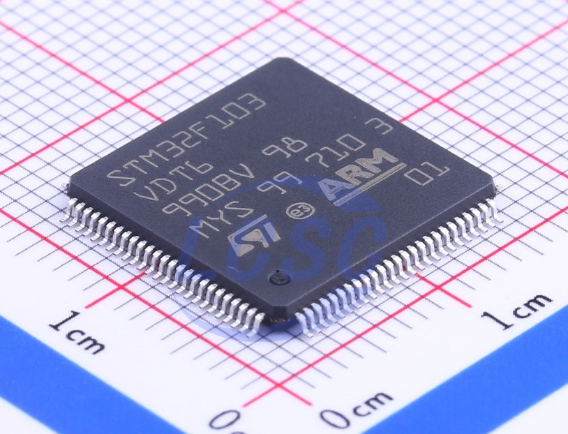
The STM32F103VDT6 in its 100-pin, 14x14mm, LQFP100 package (Image courtesy of LCSC Electronics)
When nothing works, you’ll be glad you have debugging capabilities
To ensure painfree debugging and programming, I included pin headers to access the SWD interface as well as a single USART. Although SWO can be used for serial output, most of my programmers don’t support it, so I generally find it easier to just connect the USART to a separate Serial<->USB converter for debug printing.
Bringing it all together
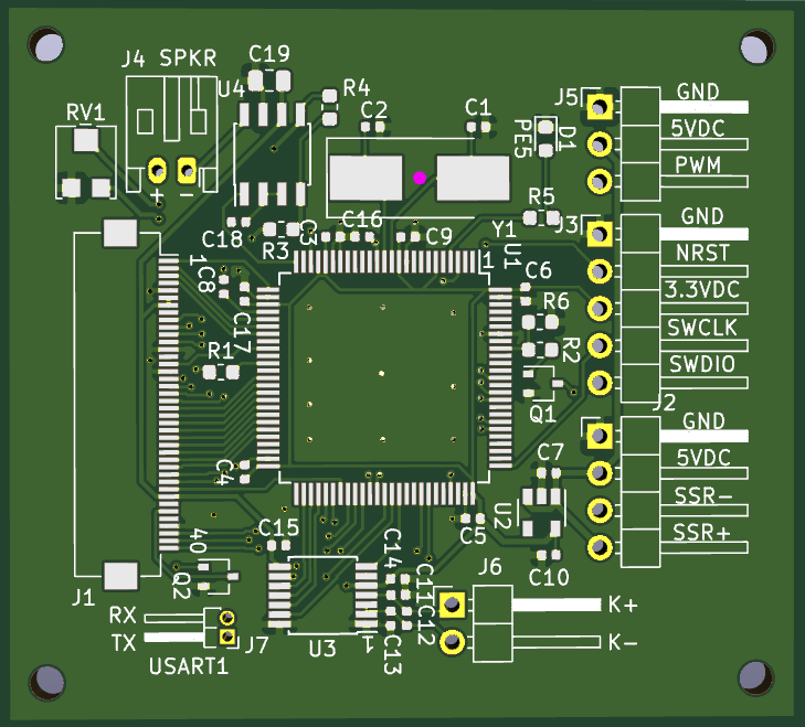
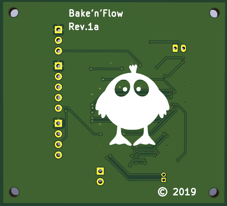
Below is the full schematic and PCB design, created in KiCad. I won’t go into detail on the PCB design; it’s pretty straightforward. The TFT LCD uses a 40-pin FPC connector, which sits at the left of the board. The audio section with a pot volume control is on the top-left and the thermocouple encoder is on the bottom. The thermocouple connector is right next to the IC to minimize thermal gradient, with all other connectors (excl. the USART and speaker) at the right side.
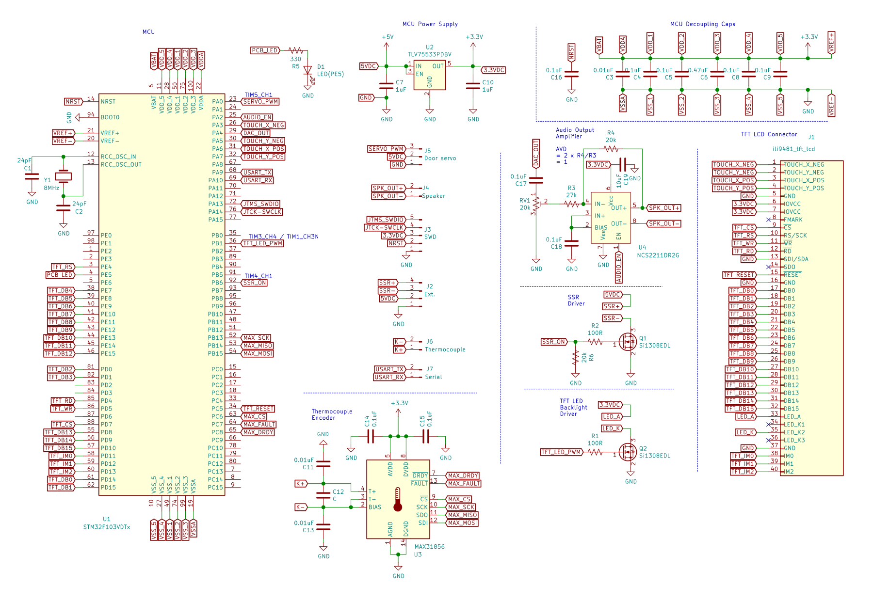
Full schematic
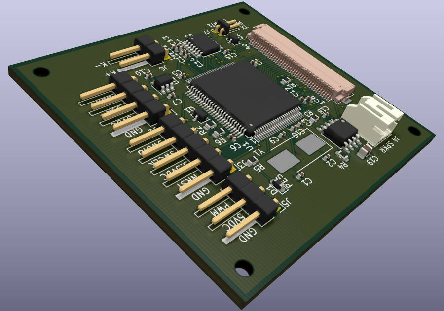
3D view of the full board
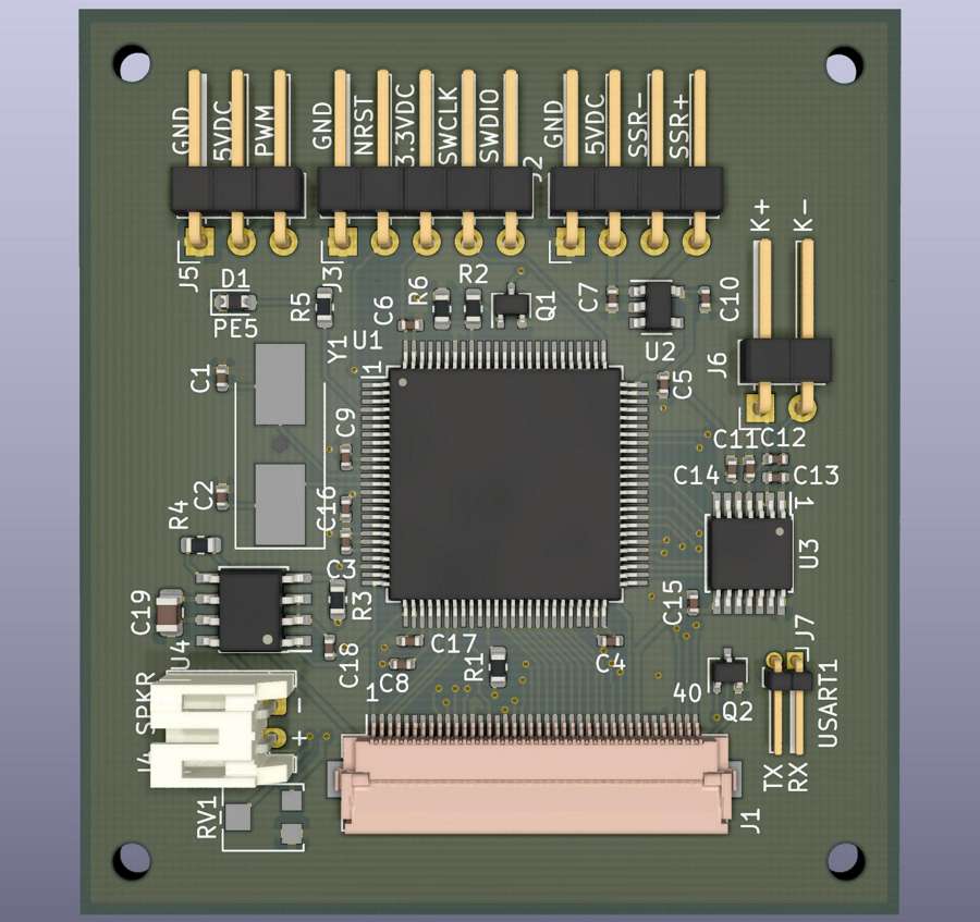
3D top view of the full board
That’s the design done. Now we need to actually make the thing. That’s the subject of the next post.

