
This is the second part of a five-part post detailing the design and implementation of new firmware for the Aqara E1 Zigbee light switches:
Any new firmware needs to know the GPIOs
After confirming that the chip had write access in ISP mode, the next step was to determine the appropriate inputs and outputs.
Specifically, the button inputs and the LED/relay outputs. The GPIOs need to be appropriately configured and setup for input/output.
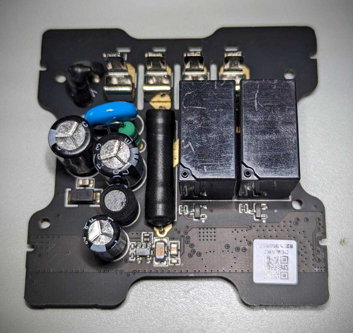
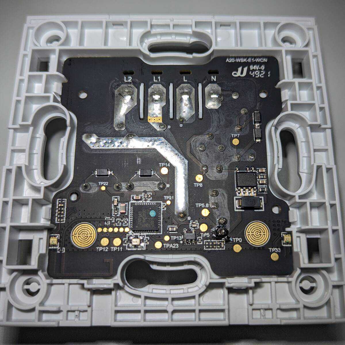
The PCB is relatively easy to access
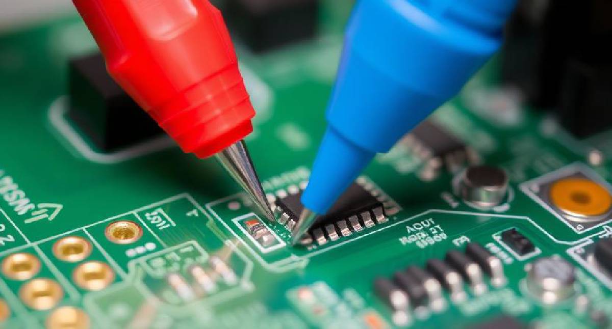
Needles are pretty conductive
After poking around the PCB with a couple of sewing needles connected to a multimeter, I produced the following - likely approximately correct - schematic:

Aqara E1 light switch schematic
Determined DIO lines
| Left | Right | Active | |
|---|---|---|---|
| Button | 11 | 10 | high |
| Blue LED | 13 | 6 | low |
| Red LED | 14 | 7 | low |
| Relay | 17 | 20 | high |
ISP access, but no debugging
The ISP programming, reset, and USART pins were readily accessible on their own pads, but the signals needed for debugging (SWDIO, SWCLK) seemed not easily connectable. SWDIO - which doubles as DIO13 - was in use as the output for the blue LED on the left button and SWDCLK appeared unconnected.
I didn’t spend much time trying to access the debug pins, as I assumed I could just get a cheap JN5189 module if I ended up needing runt-time debugging.
Update
In the end I didn’t need debug access, and developed everything with only UART logging (and error codes via LED) for debug output.
Next step - planning what features we need in firmware.